
1. Vấn đề: cấp nguồn cho nhiều module rất dễ rối
Nếu bạn làm IoT/Robot theo kiểu ráp nhiều module (GPS, SIM 4G, OLED, NRF24L01, cảm biến), phần dây nguồn thường gây khó chịu nhất:
- Mỗi module cần 2 dây VCC và GND
- Hàn nhiều điểm dễ bong pad, dễ nhầm cực
- Khi debug hoặc thay module, dây nguồn lằng nhằng khó kiểm
Giải pháp đơn giản nhưng cực hiệu quả là làm một Power Bus trên PCB:
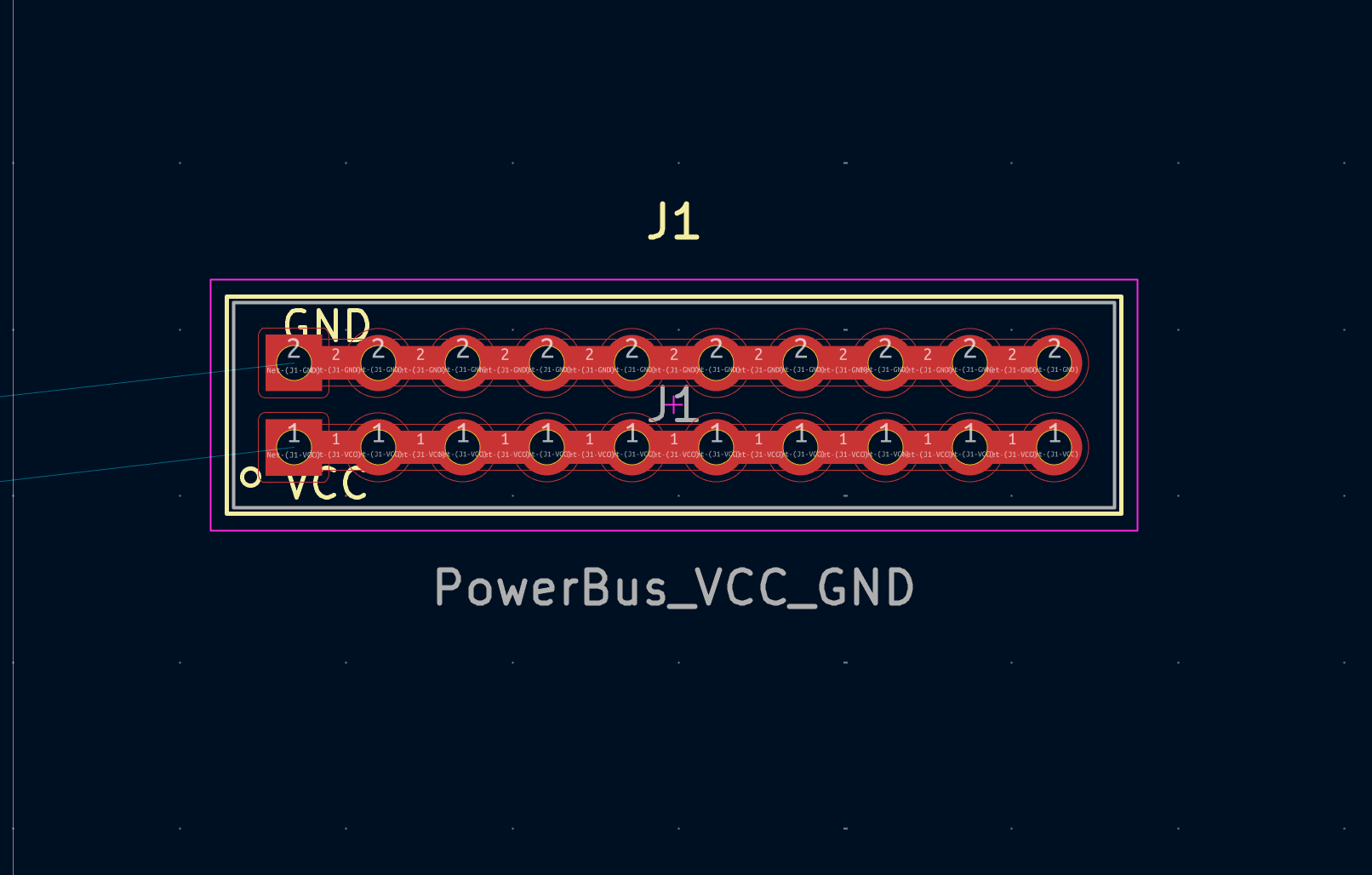
- Hàng 1: VCC có 10 lỗ, nối chung với nhau
- Hàng 2: GND có 10 lỗ, nối chung với nhau
Bạn chỉ cần hàn 2 dây vào VCC và GND một lần, sau đó muốn cấp nguồn cho module nào thì cắm/hàn vào bất kỳ lỗ nào là xong.
2. Mục tiêu kỹ thuật của Power Bus
Thiết kế Power Bus chuẩn nên đạt các tiêu chí:
- 2 hàng sát nhau để hàn gọn
- Mỗi hàng 10 lỗ (pitch 2.54mm) để dễ dùng header phổ thông
- VCC hàng 1 nối sẵn với nhau bằng copper
- GND hàng 2 nối sẵn với nhau bằng copper
- Dễ tái sử dụng: có symbol + footprint trong thư viện KiCad
3. Cách làm đúng trong KiCad: tạo Symbol + Footprint
Để dùng ổn định và không bị lỗi pin pad, bạn nên tạo cả:
- Symbol: 2 chân VCC và GND
- Footprint: 2 hàng 10 lỗ, đã có copper nối sẵn trong footprint
Quan trọng:
- Pin number của symbol phải khớp pad number trong footprint
- VCC dùng pin/pad số 1
- GND dùng pin/pad số 2
4. Tạo Symbol Power Bus (2 pin)
4.1 Tạo thư viện symbol
- Schematic Editor → Symbol Editor
- File → New Library
- Lưu tên ví dụ: IoTLabs_PowerBus_2x10_VCC_GND.kicad_sym
(kicad_symbol_lib
  (version 20231120)
  (generator "IoTLabs")

  (symbol "IoTLabs_PowerBus_2x10_VCC_GND"
    (in_bom yes)
    (on_board yes)

    (property "Reference" "J" (at 0 3.81 0) (effects (font (size 1.27 1.27) (thickness 0.15))))
    (property "Value" "IoTLabs_PowerBus_2x10_VCC_GND" (at 0 -3.81 0) (effects (font (size 1.27 1.27) (thickness 0.15))))
    (property "Footprint" "IoTLabs_Power:IoTLabs_PowerBus_2x10_VCC_GND" (at 0 0 0) (effects (font (size 1.27 1.27) (thickness 0.15))))
    (property "Datasheet" "" (at 0 0 0) (effects (font (size 1.27 1.27) (thickness 0.15))))
    (property "Description" "Power bus: 2 rows x 10 holes. Row1 VCC (all tied), Row2 GND (all tied)." (at 0 0 0) (effects (font (size 1.27 1.27) (thickness 0.15))))

    (symbol "IoTLabs_PowerBus_2x10_VCC_GND_1_1"
      (unit 1)
      (body_style default)
      (rectangle (start -5.08 2.54) (end 5.08 -2.54) (stroke (width 0.254) (type default)) (fill (type none)))

      (pin power_in line (at -7.62 1.27 0) (length 2.54)
        (name "VCC" (effects (font (size 1 1) (thickness 0.15))))
        (number "1" (effects (font (size 1 1) (thickness 0.15))))
      )
      (pin power_in line (at -7.62 -1.27 0) (length 2.54)
        (name "GND" (effects (font (size 1 1) (thickness 0.15))))
        (number "2" (effects (font (size 1 1) (thickness 0.15))))
      )
    )
  )
)
4.2 Tạo symbol mới
- File → New Symbol
- Tên gợi ý: IoTLabs_PowerBus_2x10_VCC_GND
- Reference Prefix: J (hoặc P)
4.3 Thêm 2 chân
- Pin 1: VCC (power_in)
- Pin 2: GND (power_in)
Gợi ý hiển thị:
- Đặt VCC phía trên, GND phía dưới
- Ký hiệu dễ nhìn, không cần vẽ chi tiết 20 chân vì mục đích của bus là cấp nguồn
5. Tạo Footprint Power Bus 2×10 có nối sẵn
5.1 Vì sao không chỉ dùng header 2×10 bình thường
Nếu bạn dùng footprint 2×10 chuẩn, 20 pad sẽ là 20 net riêng.
Bạn vẫn phải tự route nối 10 pad VCC và 10 pad GND, mất thời gian và dễ quên.
Vì vậy ta tạo footprint có sẵn “bus copper” để:
- VCC row tự nối với nhau
- GND row tự nối với nhau
5.2 Cách nối sẵn trong footprint (mẹo quan trọng)
Mẹo đơn giản nhất là:
- Tất cả lỗ của hàng VCC đều mang cùng pad number = 1
- Tất cả lỗ của hàng GND đều mang cùng pad number = 2
- Thêm các pad SMD “cầu nối” giữa các lỗ kề nhau để tạo copper liên tục
Nhờ vậy:
- KiCad hiểu tất cả pad VCC là cùng một chân (pin 1)
- KiCad hiểu tất cả pad GND là cùng một chân (pin 2)
- Copper đã có sẵn, bạn không cần route gì thêm
5.3 Thông số đề xuất
- Pitch theo chiều dài: 2.54mm
- Khoảng cách 2 hàng: 2.54mm (hai hàng sát nhau, dễ hàn)
- Drill: 1.0mm
- Pad: 1.7mm hoặc 1.8mm
IoTLabs_PowerBus_2x10_VCC_GND.kicad_mod
(footprint "IoTLabs_PowerBus_2x10_2.54_VCC_GND"
  (version 20240115)
  (generator "pcbnew")
  (layer "F.Cu")
  (descr "IoTLabs Power Bus 2x10: Row1 VCC (tied), Row2 GND (tied), 2.54mm pitch")
  (tags "IoTLabs powerbus VCC GND 2xN 2.54mm")
  (attr through_hole)

  (fp_text reference "J?" (at 0 -5.5 0) (layer "F.SilkS") (effects (font (size 1 1) (thickness 0.15))))
  (fp_text value "IoTLabs_PowerBus_2x10_2.54_VCC_GND" (at 0 5.5 0) (layer "F.Fab") (effects (font (size 1 1) (thickness 0.15))))
  (fp_text user "${REFERENCE}" (at 0 0 0) (layer "F.Fab") (effects (font (size 1 1) (thickness 0.12))))

  (fp_line (start -10.89 -3.27) (end 10.89 -3.27) (stroke (width 0.12) (type solid)) (layer "F.SilkS"))
  (fp_line (start 10.89 -3.27) (end 10.89 3.27) (stroke (width 0.12) (type solid)) (layer "F.SilkS"))
  (fp_line (start 10.89 3.27) (end -10.89 3.27) (stroke (width 0.12) (type solid)) (layer "F.SilkS"))
  (fp_line (start -10.89 3.27) (end -10.89 -3.27) (stroke (width 0.12) (type solid)) (layer "F.SilkS"))
  (fp_text user "VCC" (at -8.09 2.37 0) (layer "F.SilkS") (effects (font (size 0.9 0.9) (thickness 0.12))))
  (fp_text user "GND" (at -8.09 -2.37 0) (layer "F.SilkS") (effects (font (size 0.9 0.9) (thickness 0.12))))
  (fp_line (start -11.39 -3.77) (end 11.39 -3.77) (stroke (width 0.05) (type solid)) (layer "F.CrtYd"))
  (fp_line (start 11.39 -3.77) (end 11.39 3.77) (stroke (width 0.05) (type solid)) (layer "F.CrtYd"))
  (fp_line (start 11.39 3.77) (end -11.39 3.77) (stroke (width 0.05) (type solid)) (layer "F.CrtYd"))
  (fp_line (start -11.39 3.77) (end -11.39 -3.77) (stroke (width 0.05) (type solid)) (layer "F.CrtYd"))
  (fp_line (start -10.69 -3.07) (end 10.69 -3.07) (stroke (width 0.1) (type solid)) (layer "F.Fab"))
  (fp_line (start 10.69 -3.07) (end 10.69 3.07) (stroke (width 0.1) (type solid)) (layer "F.Fab"))
  (fp_line (start 10.69 3.07) (end -10.69 3.07) (stroke (width 0.1) (type solid)) (layer "F.Fab"))
  (fp_line (start -10.69 3.07) (end -10.69 -3.07) (stroke (width 0.1) (type solid)) (layer "F.Fab"))
  (fp_circle (center -10.19 2.17) (end -9.94 2.17) (stroke (width 0.12) (type solid)) (fill none) (layer "F.SilkS"))
  (pad "1" thru_hole rect (at -8.89 1.27) (size 1.7 1.7) (drill 1.0) (layers "*.Cu" "*.Mask"))
  (pad "1" thru_hole circle (at -6.35 1.27) (size 1.7 1.7) (drill 1.0) (layers "*.Cu" "*.Mask"))
  (pad "1" thru_hole circle (at -3.81 1.27) (size 1.7 1.7) (drill 1.0) (layers "*.Cu" "*.Mask"))
  (pad "1" thru_hole circle (at -1.27 1.27) (size 1.7 1.7) (drill 1.0) (layers "*.Cu" "*.Mask"))
  (pad "1" thru_hole circle (at 1.27 1.27) (size 1.7 1.7) (drill 1.0) (layers "*.Cu" "*.Mask"))
  (pad "1" thru_hole circle (at 3.81 1.27) (size 1.7 1.7) (drill 1.0) (layers "*.Cu" "*.Mask"))
  (pad "1" thru_hole circle (at 6.35 1.27) (size 1.7 1.7) (drill 1.0) (layers "*.Cu" "*.Mask"))
  (pad "1" thru_hole circle (at 8.89 1.27) (size 1.7 1.7) (drill 1.0) (layers "*.Cu" "*.Mask"))
  (pad "2" thru_hole rect (at -8.89 -1.27) (size 1.7 1.7) (drill 1.0) (layers "*.Cu" "*.Mask"))
  (pad "2" thru_hole circle (at -6.35 -1.27) (size 1.7 1.7) (drill 1.0) (layers "*.Cu" "*.Mask"))
  (pad "2" thru_hole circle (at -3.81 -1.27) (size 1.7 1.7) (drill 1.0) (layers "*.Cu" "*.Mask"))
  (pad "2" thru_hole circle (at -1.27 -1.27) (size 1.7 1.7) (drill 1.0) (layers "*.Cu" "*.Mask"))
  (pad "2" thru_hole circle (at 1.27 -1.27) (size 1.7 1.7) (drill 1.0) (layers "*.Cu" "*.Mask"))
  (pad "2" thru_hole circle (at 3.81 -1.27) (size 1.7 1.7) (drill 1.0) (layers "*.Cu" "*.Mask"))
  (pad "2" thru_hole circle (at 6.35 -1.27) (size 1.7 1.7) (drill 1.0) (layers "*.Cu" "*.Mask"))
  (pad "2" thru_hole circle (at 8.89 -1.27) (size 1.7 1.7) (drill 1.0) (layers "*.Cu" "*.Mask"))
  (pad "1" smd rect (at -7.62 1.27) (size 1.6 1.0) (layers "*.Cu" "*.Mask"))
  (pad "1" smd rect (at -5.08 1.27) (size 1.6 1.0) (layers "*.Cu" "*.Mask"))
  (pad "1" smd rect (at -2.54 1.27) (size 1.6 1.0) (layers "*.Cu" "*.Mask"))
  (pad "1" smd rect (at 0 1.27) (size 1.6 1.0) (layers "*.Cu" "*.Mask"))
  (pad "1" smd rect (at 2.54 1.27) (size 1.6 1.0) (layers "*.Cu" "*.Mask"))
  (pad "1" smd rect (at 5.08 1.27) (size 1.6 1.0) (layers "*.Cu" "*.Mask"))
  (pad "1" smd rect (at 7.62 1.27) (size 1.6 1.0) (layers "*.Cu" "*.Mask"))
  (pad "2" smd rect (at -7.62 -1.27) (size 1.6 1.0) (layers "*.Cu" "*.Mask"))
  (pad "2" smd rect (at -5.08 -1.27) (size 1.6 1.0) (layers "*.Cu" "*.Mask"))
  (pad "2" smd rect (at -2.54 -1.27) (size 1.6 1.0) (layers "*.Cu" "*.Mask"))
  (pad "2" smd rect (at 0 -1.27) (size 1.6 1.0) (layers "*.Cu" "*.Mask"))
  (pad "2" smd rect (at 2.54 -1.27) (size 1.6 1.0) (layers "*.Cu" "*.Mask"))
  (pad "2" smd rect (at 5.08 -1.27) (size 1.6 1.0) (layers "*.Cu" "*.Mask"))
  (pad "2" smd rect (at 7.62 -1.27) (size 1.6 1.0) (layers "*.Cu" "*.Mask"))
)
6. Add Power Bus vào thư viện IoTLabs
6.1 Add symbol library
Schematic Editor → Preferences → Manage Symbol Libraries
- Add file IoTLabs_Power.kicad_sym
- Nickname: IoTLabs_Power
6.2 Add footprint library
PCB Editor → Preferences → Manage Footprint Libraries
- Add folder IoTLabs_Power.pretty
- Nickname: IoTLabs_Power
7. Cách dùng Power Bus trong project
- Đặt symbol Power Bus lên schematic
- Nối pin VCC vào net VCC (hoặc +3V3 tuỳ bạn đặt tên)
- Nối pin GND vào net GND
- Gán footprint: IoTLabs_Power:IoTLabs_PowerBus_2x10_VCC_GND
- Update PCB from Schematic
Khi ra PCB:
- Bạn sẽ thấy 2 hàng 10 lỗ
- Hàng VCC nối sẵn
- Hàng GND nối sẵn
Giờ bạn chỉ cần:
- Hàn nguồn vào 1 lỗ VCC và 1 lỗ GND
- Các module khác muốn lấy nguồn thì hàn/cắm vào bất kỳ lỗ nào
8. Lưu ý thực chiến để bus nguồn “không tụt áp”
Nếu bạn cấp cho các module ăn dòng lớn (ví dụ SIM 4G), bạn nên:
- Tăng bề rộng copper nối bus (cầu nối SMD lớn hơn)
- Ưu tiên đổ đồng GND plane toàn board
- Đặt tụ lọc gần module ăn dòng lớn
9. Kết bài
Power Bus là một chi tiết nhỏ nhưng giúp dự án gọn gàng hơn rất nhiều.
Nó đặc biệt hữu ích trong các board IoTLabs, nơi bạn luôn cần cấp nguồn nhanh cho nhiều module trong giai đoạn test, debug và nâng cấp.
Bonus:
Fle mẫu Symbol + Footprint:
Cách dùng nhanh:
- Tạo folder
IoTLabs_Power.pretty/và bỏ file.kicad_modvào đó. - Add
IoTLabs_Power.kicad_symtrong Manage Symbol Libraries - Add folder
IoTLabs_Power.prettytrong Manage Footprint Libraries - Trong schematic đặt symbol IoTLabs_PowerBus_2x10_VCC_GND, nối VCC/GND là xong.
Footprint này có sẵn “cầu nối” copper giữa các lỗ nên 10 lỗ VCC nối chung và 10 lỗ GND nối chung dễ sử dụng.
Leave a Reply